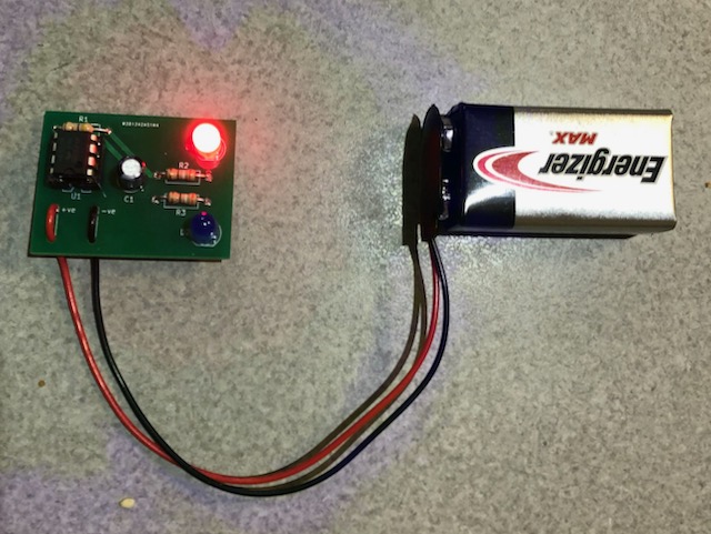
From design to PCB
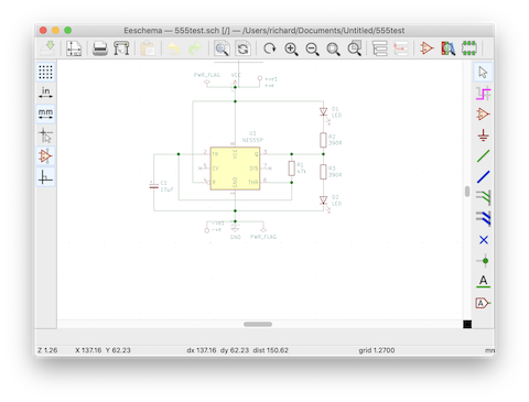
This year with students back in the classroom it was time to resume the development process. I was able to use a professional development day in Term 2 to finally get to grips with KiCad. I had already looked at a tutorial so using that as a reference I started the process to turn this circuit into a finished PCB that I could use in classes.
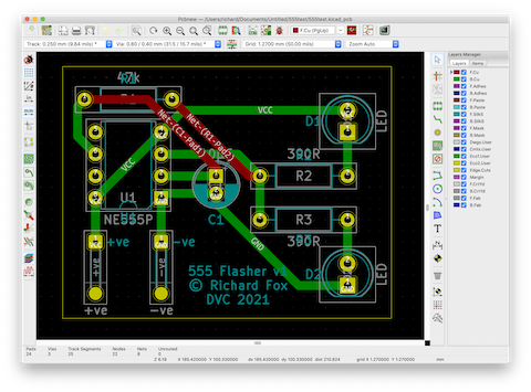
Following the steps in the KiCad tutorial I was able to create the circuit, then export this to a board design, choosing the appropriate footprints for components. Next step was to do the layout and connect up the tracks.
KiCad has a very neat 3D viewer which means you can view a finished board before it even gets produced.
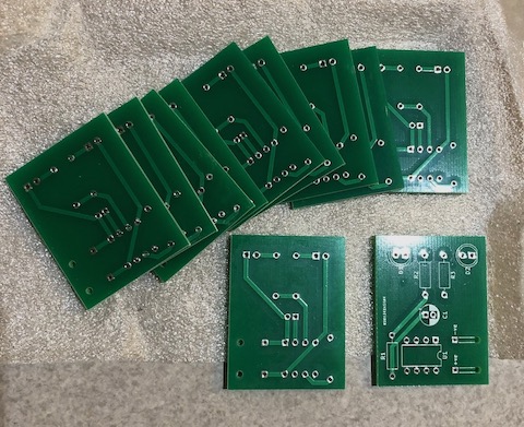
Previously I had ordered some PCBs from others’ designs from PCBWay as a test. From KiCad I was able to export my board layers as Gerber files. PCBWay has a quick feature where you just upload the Gerber files and it does all of the configuration. Their prototype rate means that you can get 10 boards made for just USD$5, but unfortunately the shipping costs rather more. Nevertheless, the service is incredibly quick, from submitting the order on Wednesday to receiving it on Monday morning, from China to Australia. The unit cost will come down when I order larger numbers for production.
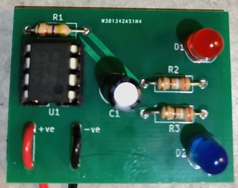
When the boards arrived, 5 minutes work with the soldering iron and a finished product.
